


Union Minister Vaishnaw inaugurates India’s first 3nm chip design centre in Noida, Bengaluru
Wed 14 May 2025, 10:06:49
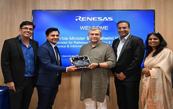
Union Minister for Electronics and Information Technology Ashwini Vaishnaw inaugurated new state-of-the-art design facilities located in Noida and Bengaluru. Highlighting the uniqueness of the new facility, Mr. Vaishnaw stated that this is India’s first design centre to work on cutting-edge 3-nanometer chip design, a milestone that firmly places India in the global league of semiconductor innovation.
Emphasising the growing momentum in India’s semiconductor ecosystem, Mr Vaishnaw announced that the inauguration of the major Semiconductor Design Centre in Uttar Pradesh is a critical step toward developing a pan-India ecosystem that harnesses the rich talent available across the country.
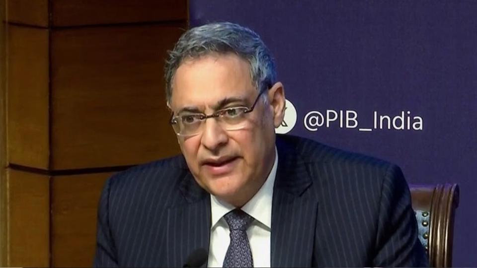
During his interaction with the media, Mr. Vaishnaw asserted that the
semiconductor ecosystem in India is progressing well, aligning with Prime Minister Narendra Modi’s vision of establishing a comprehensive semiconductor ecosystem in the country. The Minister highlighted that a key feature of this centre is its capability to design 3-nanometer chips, among the most advanced in the world, end-to-end within India, marking a first for the nation.
semiconductor ecosystem in India is progressing well, aligning with Prime Minister Narendra Modi’s vision of establishing a comprehensive semiconductor ecosystem in the country. The Minister highlighted that a key feature of this centre is its capability to design 3-nanometer chips, among the most advanced in the world, end-to-end within India, marking a first for the nation.
Mr Vaishnaw also announced the launch of a new semiconductor learning kit aimed at enhancing practical hardware skills among engineering students. He also stated that 270+ academic institutions that have already received advanced EDA Electronic Design Automation (EDA) software tools under the India Semiconductor Mission will also receive these hands-on hardware kits.
No Comments For This Post, Be first to write a Comment.
Most viewed from National


Most viewed from World


Todays Epaper

English Weekly


AIMIM News


Latest Urdu News
Most Viewed
May 26, 2020
Which cricket team is your favourite to win the T20 World Cup 2026?
Latest Videos View All
.jpg)
.jpg)
.jpg)


Like Us
Home
About Us
Advertise With Us
All Polls
Epaper Archives
Privacy Policy
Contact Us
Download Etemaad App
© 2026 Etemaad Daily News, All Rights Reserved.